
Introduction
Optimize for EMC emission and immunity and don't forget all the others.
A printed circuit board (PCB) normally operates in a 3-dimensional electromagnetic environment. Several cable connections will cross other electromagnetic domains.
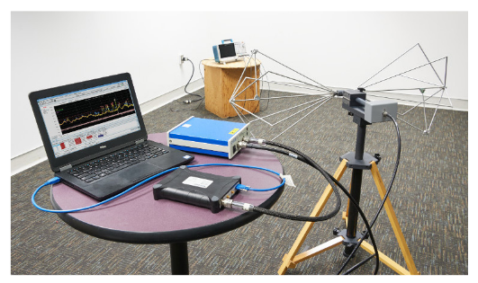 Typical EMC emission test (Tektronics).
EMC specialists tend to focus on only one aspect, the EMC validation test, but that’s not how it works. Electronic designs might pass all the EMC validation tests, but still suffer from clock-jitter, self-pollution and software hang-ups. This results in designs that have a low technical performance and are extremely difficult to maintain.
In a professional and demanding world this is not acceptable.
Electronic hardware design
Preventing electronic design self-polution, because it's important!
The picture shows a self-polluted (oversampling) ADC system of 24 bits.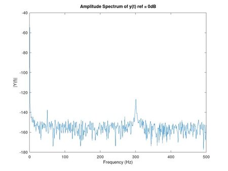 Pollution visible in the FFT noise-floor-spectrum shows two peaks coming up at 50Hz and 300Hz. The 50Hz is the mains frequency leaking into the measurement system, while the 300Hz is caused by self-pollution of the electronics. The 24-bit ADC system is therefore limited to a dynamic range of 20-bits. This is caused by improper PCB design, bad layout and a lack of noise-class-partitioning. Because a total bandwidth of 0-500Hz was required, filtering and further digital processing was not possible. So unfortunately, a redesign using proper noise-class patitioning was necessary.
Signal and Power integrity
And mixed system specialization.
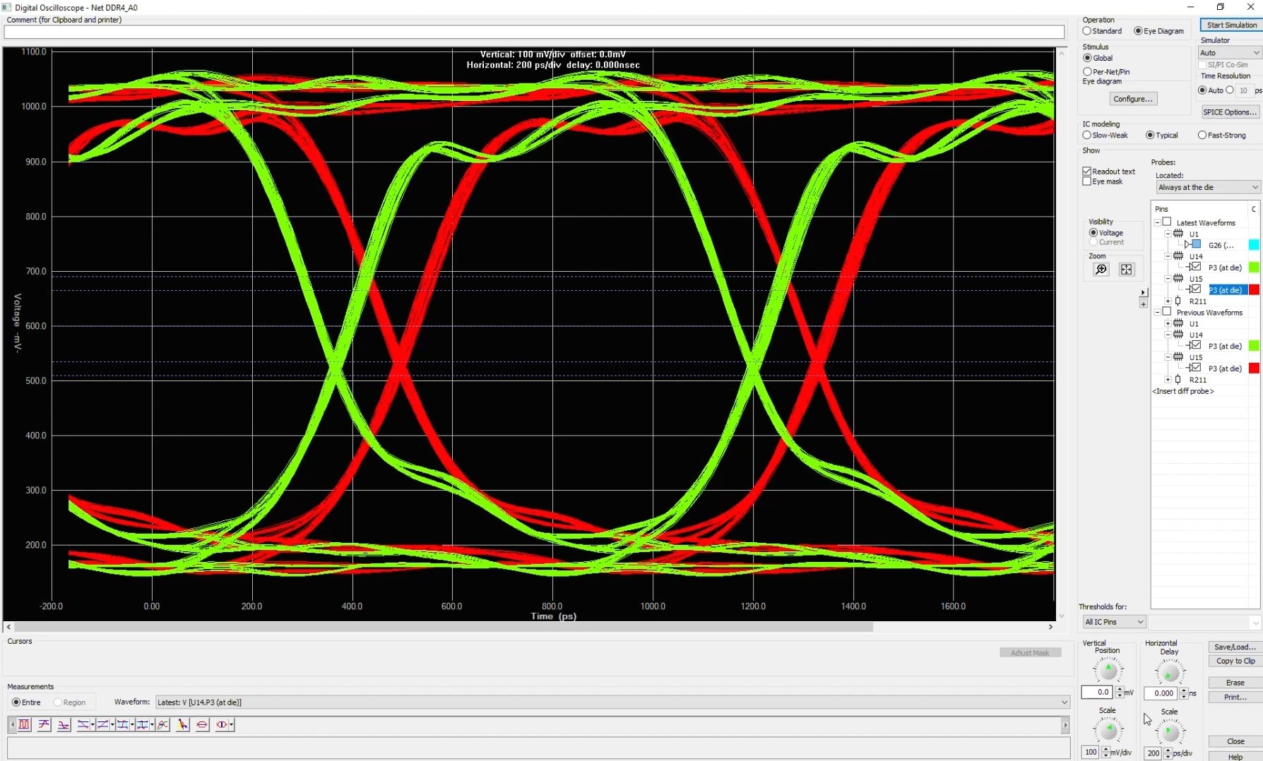 Typical simulated signal (Hyperlynx).
Modern electronic components often have very fast edges due to the technology used. As a result, these signals contain high frequencies and the PCB tracks behave like transmission lines. If these PCB tracks are not routed properly, this will result in problematic and unreliable electronics. this craftsmanship is called "signal integrity".
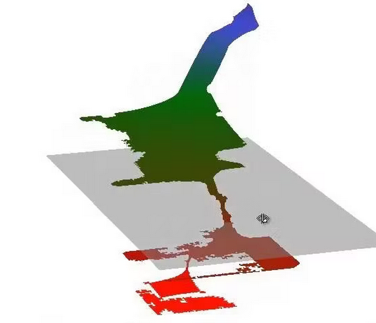 DC drop of voltage (Hyperlynx).
Because of this high frequency, the power supply must be able to supply a lot of current quickly. Sometimes current densities play a dominant role. Issues such as current displacement and voltage drops become a major problem. This subject is called "power integrity". It is important to have insight into these matters for the development of reliable electronics. More than 25 years of experience in the development of printed circuit boards with fast signals. Often professional designs, sometimes large volumes for consumer electronics. Simulation of this electronics is a must. Things like "best engineering practice" and "guts feeling" are no longer sufficient here.The behavior of these fast sinals and of the power distribution is often contrary to intuition.
About me
Jack Leijssen
30+ Years of experience in the field of extreme EMC demanding electronics and PCB designs.
Read the full article in the Bits&Chips. and this one.
Dutch article in the Hightechsystems.
“The IC designers screwed up and I got to clean up their mess,” recounts Jack. “They failed to adequately separate the analog and digital parts on the chip. Fixing that was not an option as that would have meant that they would have to start all over again.
 Oktober 2024
I had to look for solutions outside the chip. Moving the power supply, for example. And with all kinds of resistors terminating the transmissionlines, I was able to curb the over and underflow currents, thereby reducing the crossover between the digital nets and improving the signal-to-noise ratio to the analog part. I fixed the IC design screwups on the board level.” With this, he cemented his reputation as an electronic design specialist within Philips. Nowadays Jack is teaching via the High Tech Institute. in the area of signal integrity, power integrity and EMC